Current Solutions
Moore’s law is the bottleneck of the performance of a single chip, thus GPU cluster is the unique future of AI training, concurrent inference and AI4S; Interconnection bandwidth BW is the NASC for the scability
Current Cluster Parallelism
- Intranode: NVLINK for 8 GPU 4Tb/s
- Internode: infiniband, 400Gb/s
- low GPU efficiency
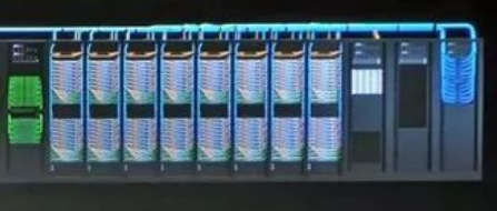
DGX GH200
- links 256 GPUs via 4x800G optics for full-speed NVLink, achieving 76% cluster efficiency.
- speeds $millions for optical modules;$6000 for each GPU
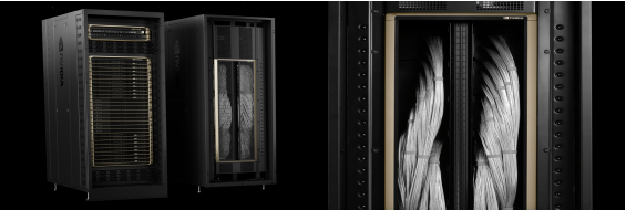
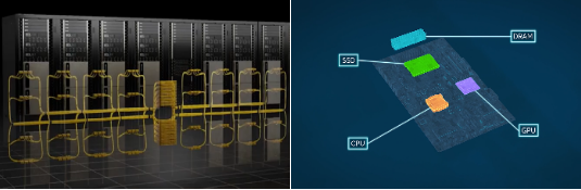
GB200 nvl72
- Custom copper backplane for 8Tb/s full-bandwidth interconnect.
- Max 72 GPUs per system. $2k/GPU.
- 120kW power challenges reliability; cooling (CDU) >$300k.